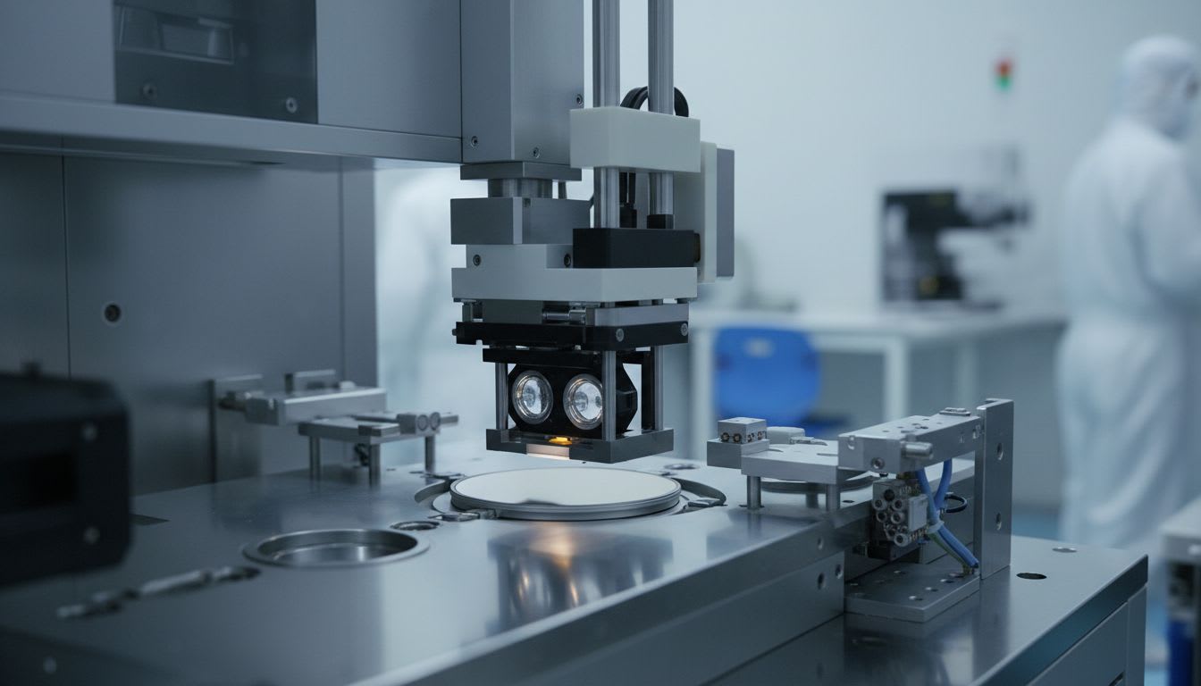
Leaders in the semiconductor industry say with one voice that reducing even the smallest process deviations is the path to pushing beyond the limits of yield. In a cleanroom environment where not even a single invisible particle of dust can be tolerated, physical transfer between processes itself carries critical contamination risks and inefficiencies.
To solve these challenges, Huvics has achieved innovation by integrating the core stages of lamination, tape mounting, and UV curing into one system. Moving beyond simple equipment adoption, let us look at why the one-stop technology from Huvics, which is fundamentally reshaping production structures on manufacturing sites, has become the most powerful strategic choice for semiconductor manufacturers.
Innovation in Semiconductor Processes, the Huvics One-Stop System
Cleanroom Environment and Process Optimization
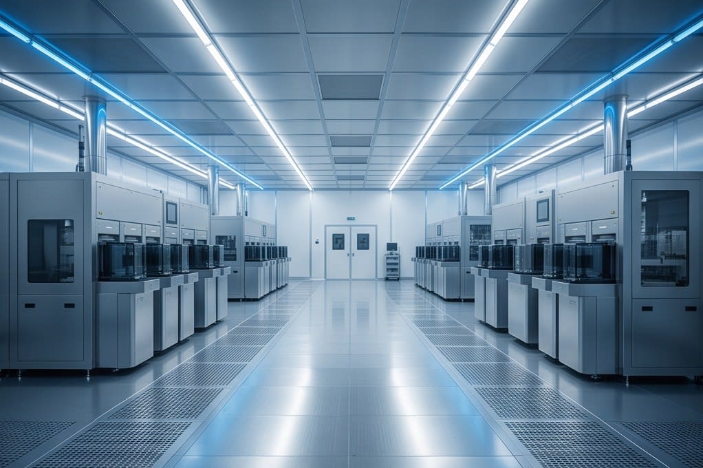
A cleanroom at a semiconductor manufacturing site is a space that requires an extreme level of cleanliness where even a tiny particle of dust cannot be allowed. Because it is a sensitive environment where just one small particle can determine overall yield, manufacturers face the challenge of securing a higher level of precision and process stability than ever before.
Key Features of the Integrated Process
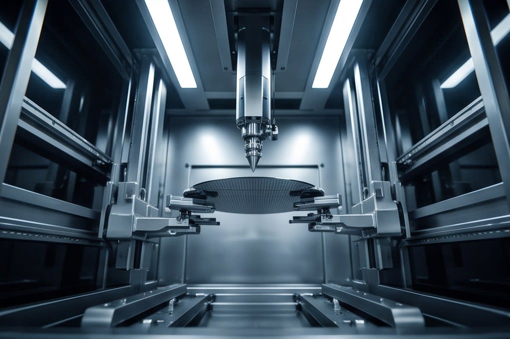
To satisfy these strict standards, Huvics has introduced a one-stop system that integrates three core processes, lamination, tape mounting, and UV curing, into a single piece of equipment. The main features of the system provided by Huvics are as follows.
- Eliminates physical transfer to block contamination risks at the source
- Implements a design that optimizes occupied space inside the cleanroom
- Enhances operational completeness and presents a standard for manufacturing efficiency
Precision Control Technology and Maximized Production Efficiency
LED-Based UV Curing Technology
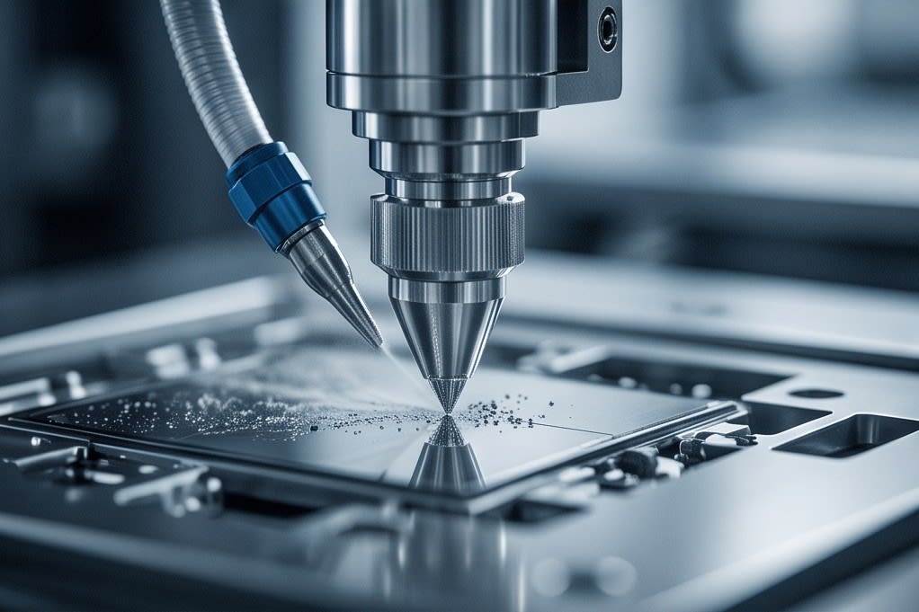
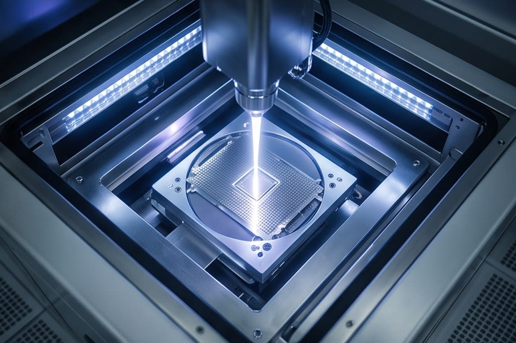
The technological differentiation of the Huvics system is concentrated in its precisely designed LED-based UV curing technology. In semiconductor assembly processes, bonding quality is a critical factor that determines the reliability of the final product, and the Huvics system delicately controls consistent light intensity and wavelength to maintain bonding strength at the most ideal level.
Reduced Defect Rate and Shortened Tact Time
This precision control capability secures the reliability of subsequent processes while dramatically lowering the defect rate. The tact time required in complex assembly lines is shortened through this efficient curing process, becoming a powerful tool for meeting the extremely demanding quality standards required by manufacturers.
Based on the belief that technology is process optimization itself, and that this optimization directly leads to manufacturer competitiveness, Huvics continues to evolve to maximize production efficiency.
Improving Cost Structure and Securing Future Competitiveness
Integrated Solution for Improving Production Efficiency
Simplifying processes goes beyond shortening work time and becomes the key to fundamentally improving a manufacturer's cost structure. By reducing the operational burden created by running multiple pieces of equipment separately and handling all core stages with a single one-stop system, production efficiency improves dramatically.
Huvics as a Strategic Choice
This integrated solution is a strategic option that enables companies to solve the challenges of cost reduction and productivity improvement in semiconductor production sites all at once. Through innovative efforts to raise process efficiency to the highest level, Huvics is building an even stronger structure for semiconductor production lines.
The technological capabilities of Huvics, which are defining new process standards for global semiconductor cleanrooms, are establishing themselves as a reliable investment and strategic choice for manufacturers seeking to secure future competitiveness.
Closing Remarks
As discussed above, the completeness of technology depends on how efficiently it compresses processes and eliminates uncertainty. The challenges of contamination risk and process delays faced by semiconductor manufacturing sites have been transformed into opportunities for optimization through the integrated solution from Huvics.
As the need to maximize production efficiency while improving cost structures becomes more important, the innovative process standard presented by Huvics will become the most reliable answer. We invite you to experience firsthand how the power of technology that precisely controls even the smallest invisible details will change the future of semiconductor manufacturing.
Huvics is an advanced technology company that develops and manufactures automation equipment and
production systems across the semiconductor, LED, Mobile, and Cosmetic industries.
With top talent and continuous technological innovation, we support customer productivity improvement and
quality competitiveness.
Huvics Contact Information
Phone: 031-374-8285
Email: cdpark@huvics.com