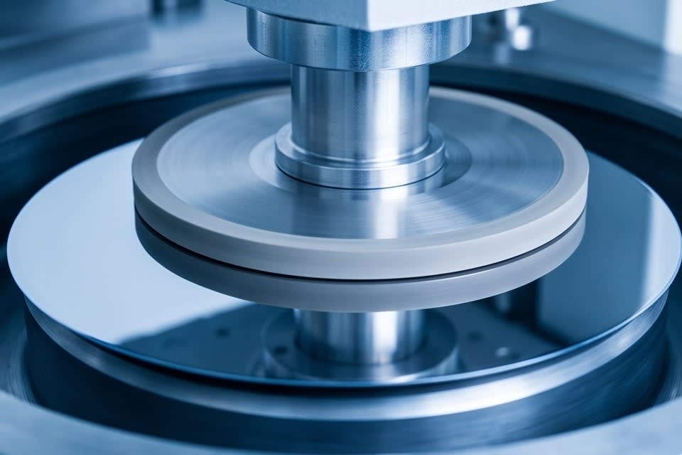
When working on a semiconductor line, even a single thickness deviation can bring down an entire day of yield. The process design is correct, and the equipment is operating normally, yet the finished thickness varies little by little. If this subtle difference is ignored, it returns as a bigger issue in the next process, and correcting it requires stopping the entire line. Even though this situation repeats itself, many sites still run the same process in the same way.
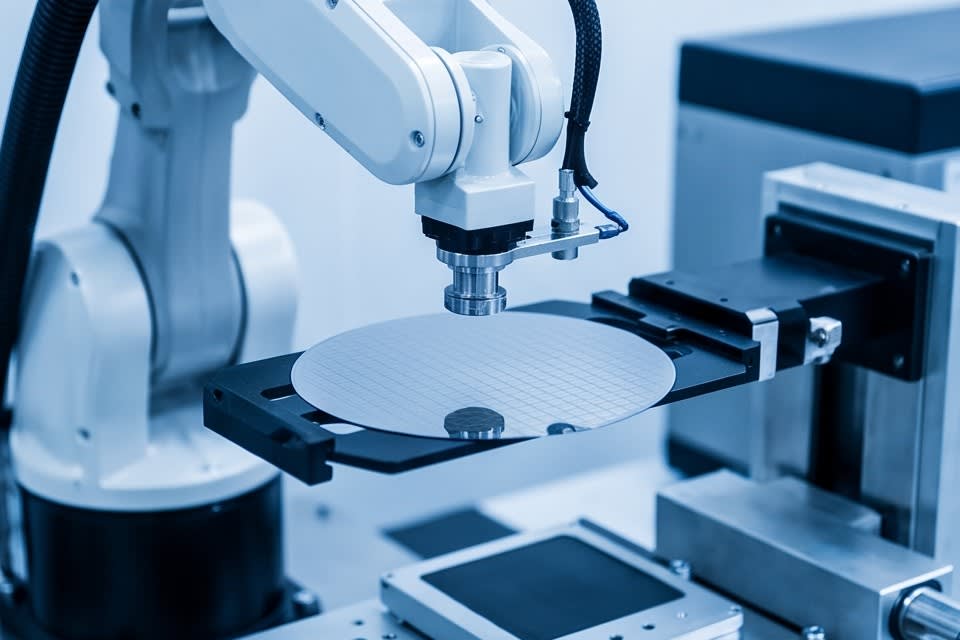
Why Thickness Uniformity Determines the Yield of Stacked Packages
In structures where dozens of chips are stacked vertically, such as AI semiconductors and high-performance memory, thickness variation in each layer is not merely a dimensional issue. As layers are stacked, deviations accumulate, and the reliability of the final package is directly affected by that accumulated value.
According to industry standards, the allowable range for thickness uniformity in production wafers is around 0.5~2.0 micrometers, and fields that require high precision, such as 5G processors and AI accelerators, require control within 0.3 micrometers. Standards stating that tolerance must remain within 1 micrometer even when the final thickness is reduced to around 20 micrometers are also being applied in actual processes.
To implement this level of precision reliably, both the stage precision of grinding equipment and the control level of the diamond wheel must be supported together. Maintaining uniform package thickness goes beyond improving the completeness of a specific process and becomes a prerequisite that determines the yield of all subsequent assembly stages. As the number of stacked layers increases, managing variation in the initial grinding stage is becoming a decisive factor in the quality of the entire process.
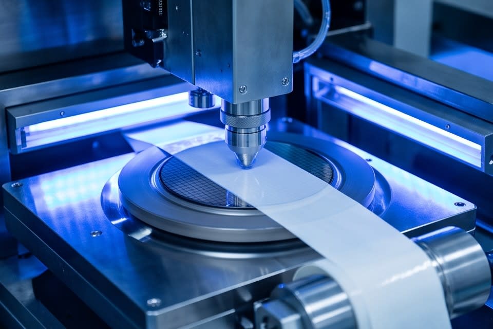
How an Integrated Laminator Structure Reduces Process Bottlenecks
When tape mounting and UV curing are operated as separate processes on the manufacturing floor, transfer time and waiting sections occur between the two pieces of equipment, and quality variables can enter during that gap. The more separated the processes are, the more management points are created, and it becomes harder to identify where bottlenecks occur.
The integrated laminator structure, which processes everything from expansion to UV curing within a single line, emerged as a way to solve this issue. Huvics' one-stop laminator system combines tape mounting and UV curing into one continuous flow, eliminating transfer sections between processes and reducing overall takt time. The LED-based UV curing method maintains stable adhesive strength while preventing adhesive defects that may occur during complex packaging assembly processes.
In the industry, comparative analyses indicate that inline UV curing systems are more efficient in high-capacity continuous production environments that require throughput of more than 500 units per hour. A structure that provides both Semi Auto and Manual options makes it possible to configure the line flexibly according to product type and production scale. How simply the process is designed becomes the key decision criterion for improving both yield and productivity.
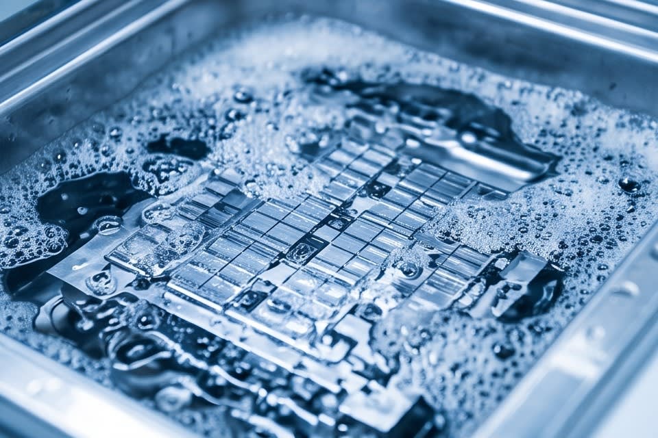
Why the Precision of Cleaning Technology Becomes the First Line of Defense for Final Quality
For components where surface cleanliness is directly linked to performance, such as camera modules and autonomous driving sensors, even a microscopic particle invisible to the naked eye can lead to a defect judgment. In semiconductor tray cleaning processes as well, residual contaminants repeatedly become sources of contamination in the next process.
Huvics' cleaning system uses a multi-stage structure that combines microbubbles, water jets, and air knives step by step, sequentially treating contaminants with various properties that are difficult to remove with a single cleaning method. In the industry, research findings have accumulated showing that micro- and nanobubble cleaning technology using bubbles with a diameter of 0.1 micrometers or less is effective in removing organic matter from semiconductor surfaces, and there are also cases where particle removal efficiency of 92.5% was confirmed in jet flow cleaning using acoustic bubble array technology.
As the applications are diverse, including camera modules, sensors, VCM motors, and trays, the system is designed for process completeness by incorporating an oven drying function that removes residual moisture after cleaning. Configurations with Full Auto and Manual options make it possible to adjust the automation level and maintenance method to suit the production environment.
Although cleaning may appear to be the final process, field data repeatedly confirms that its results become the first line of defense for final quality. This is where the precision of technology that captures a single particle determines the meaning of finished product reliability.
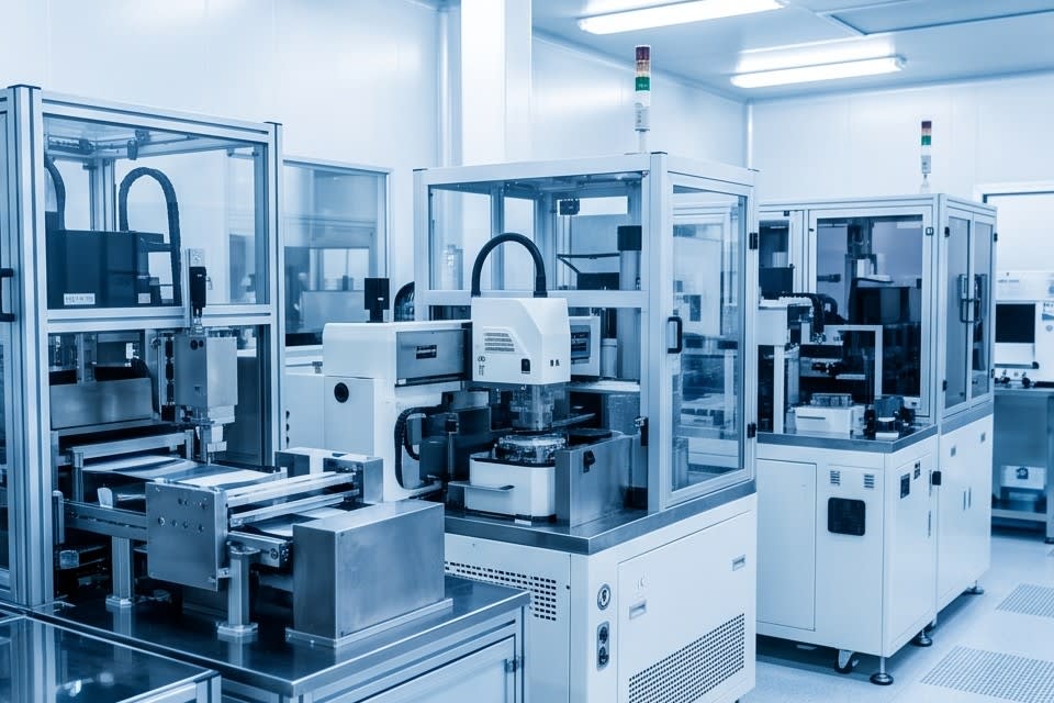
The minute thickness deviation that first caused the line to stop is, in fact, not a gap in process design but the result of precision levels at each stage failing to work together. When grinding uniformity, lamination integration efficiency, and multi-stage cleaning completeness are connected as one flow, the causes of repeated defects finally disappear. The industrial standard created by ultra-precision machining is determined not by the performance of a single piece of equipment, but by how tightly the entire process is connected.
Huvics is an advanced technology company that develops and manufactures automation equipment and
production systems across the semiconductor, LED, Mobile, and Cosmetic industries.
With top talent and continuous technological innovation, we support customers in improving productivity and
securing quality competitiveness.
Huvics Contact
Phone: 031-374-8285
Email: cdpark@huvics.com