Are you dismissing the minor contamination occurring in the AI semiconductor production process as insignificant? If left unchecked because it is invisible, it may slow down production speeds slightly at first, but in the long run, it can lead to the following issues:
- Productivity decline and quality issues due to increased defect rates
- Rework and disposal costs leading to massive financial losses
- An unforeseen crisis resulting in a decline in company credibility
Huvics offers the optimal cleaning solution to address these potential risks and allow our clients to operate their AI semiconductor production lines more safely and efficiently.
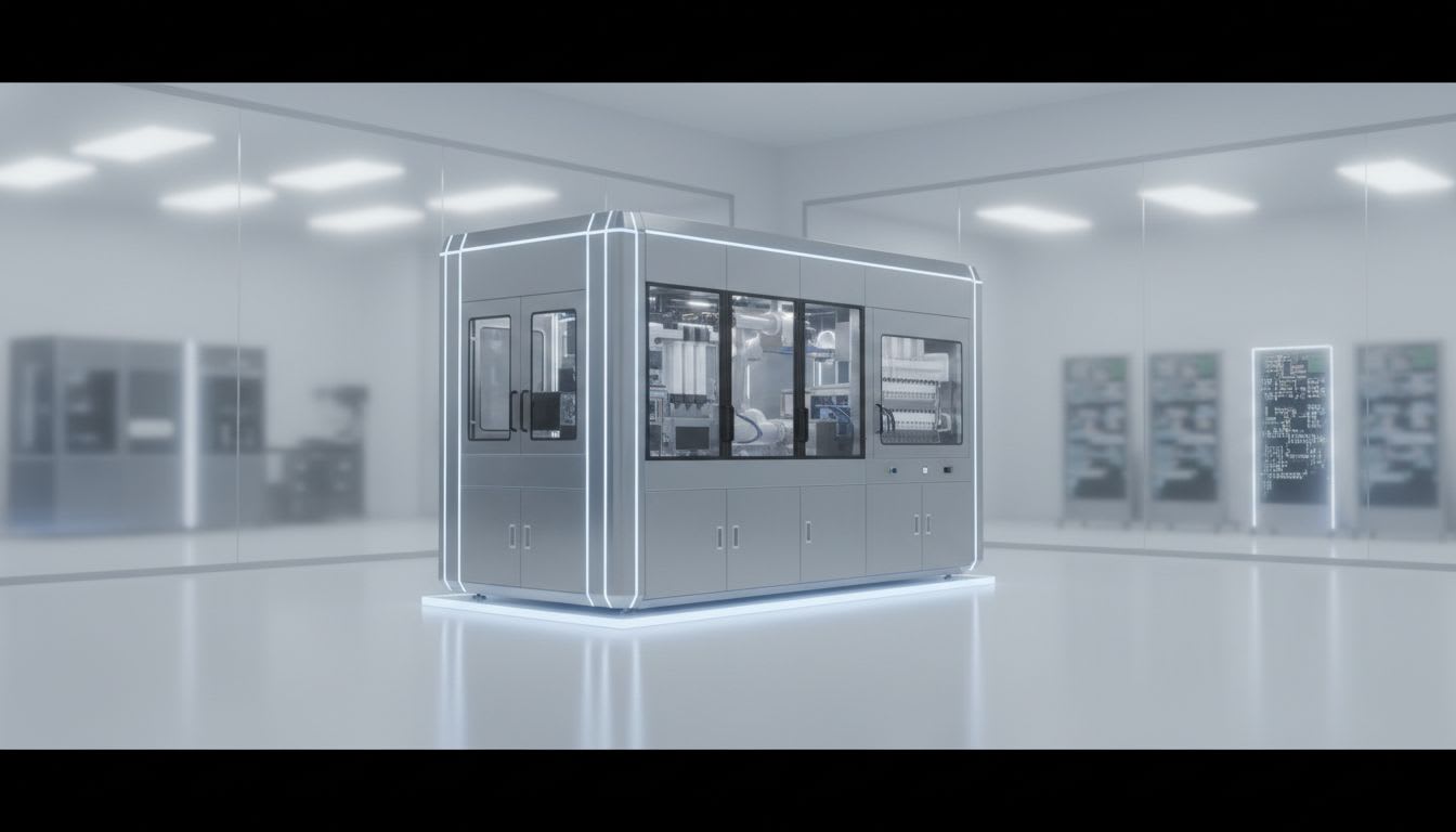
AI Semiconductor Cleaning's Core: Micro Bubble and Water Jet
Principles and Advantages of Micro Bubble Cleaning
In the forefront of AI semiconductor production, cleaning technology is a critical factor that directly relates to the performance of the final product, transcending a mere process. This is because the complex structure of AI semiconductors, which are miniaturized from micron to nano scale, can lead to fatal defects from even a small particle of contamination. Against this backdrop, micro bubble cleaning excels by penetrating deeply into the gaps of micro-patterns on the wafer surface, using micro bubbles sized from hundreds of microns to a few nanometers, to gently separate contaminants like a precision spa ampoule removing impurities deep within the skin. This provides excellent cleaning effects while minimizing physical impact, making it ideal for high-density AI semiconductor circuits that are extremely sensitive to surface damage, significantly reducing the risk of wafer damage, decreasing defect rates, and increasing production yield.
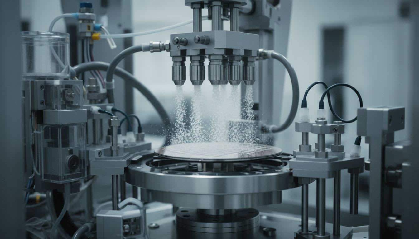
Features and Strengths of Water Jet Cleaning
On the other hand, water jet cleaning presents the following strengths:
- Effectively removes large particle contaminants and residues adhered to the surface with powerful water pressure
- Increases efficiency for high-volume production with swift contaminant processing during manufacturing
Huvics deeply acknowledges the importance of these two cleaning technologies, providing a multi-step cleaning solution optimized for the client's AI semiconductor production environment, helping reduce defect rates and guaranteeing final quality stability.
Criteria for Choosing Optimal Cleaning Technology: Target Characteristics and Yield Goals
Core Criteria for Cleaning Technology Selection
Each cleaning technology has its unique strengths. So, what criteria should our company use to make the best choice for AI semiconductor production? The key is to clearly define the 'characteristics of the cleaning target' and the 'final yield goals'.
For example, with high-performance AI semiconductor wafers that have extremely detailed and complex patterns, precision is crucial for cleaning. In this case, micro bubble cleaning, which removes fine contaminants without physical damage, is far more advantageous in ensuring wafer integrity and maximizing final yield. Minimizing the risk of surface damage, reducing the likelihood of malfunctions or damage to fine circuits, is important.
Conversely, for processes where patterns are relatively less complex or where larger particle contaminants need rapid removal, the powerful cleaning capability of water jet technology can be a more efficient solution. Huvics does not stubbornly adhere to a single cleaning technology, but instead proposes customized cleaning solutions by thoroughly analyzing the product type, production environment, and required yield goals. Properly understanding our product's characteristics and choosing the optimal cleaning method is key to securing competitiveness in the AI semiconductor market.
Choosing Cleaning Technology from a Long-term Perspective: Total Cost of Ownership (TCO) Analysis
TCO Analysis of Water Jet Cleaning
In addition to considering the characteristics of the cleaning target and the yield goals, choosing a cleaning technology should be a strategic decision, not based solely on initial investment costs. Water jet cleaning's relatively low initial equipment cost and rapid cleaning capability are clear strengths. However, the possibility of micro physical impacts on the wafer surface from high water pressure is an unignorable risk factor for sensitive products like AI semiconductors. Such micro damages, though not immediately noticeable, can lead to increased defect rates and reduced yield in the long run, acting as 'hidden costs' that ultimately raise production costs.
Long-term Economics of Micro Bubble Cleaning
Conversely, the initial investment cost of micro bubble cleaning may be higher. However, by minimizing wafer damage and achieving high yields, it can be a much more economical choice in the long term. This improves final product quality stability, enhances client market credibility, and reduces rework and disposal costs. From the perspective of total cost of ownership (TCO), Huvics thoroughly analyzes the pros and cons of each cleaning technology, providing solutions that align with the client's production goals and long-term vision. Beyond simply equipment sales, Huvics aims to be a steadfast partner in the sustainable growth and technological innovation of the client's successful future in AI semiconductor production.
In AI semiconductor production, the choice of cleaning technology transcends mere process, being a key strategic decision that mitigates potential losses, ensures high yield, and enhances market competitiveness. Understanding the clear differences in the sensitivity of micro bubbles and the strength of water jets, and finding the optimal method that most aligns with our product's characteristics and goals, is crucial. As a reliable partner to solve these concerns, Huvics provides customized multi-step cleaning solutions, guiding the way to stable, high-quality AI semiconductor production. Now is the time to confidently select the best choice and seize the future of the AI semiconductor market.
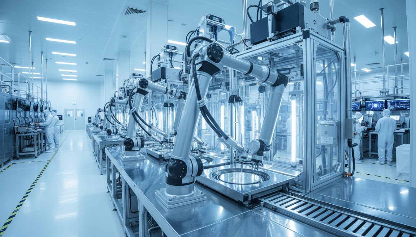
Huvics is a high-tech company developing and manufacturing automation equipment and
production systems across the semiconductor, LED, Mobile, and Cosmetic industries.
With top-tier talents and continuous technological innovation, we support clients in improving productivity and
securing quality competitiveness.
Contact Huvics Co., Ltd.
Phone: 031-374-8285
Email: cdpark@huvics.com