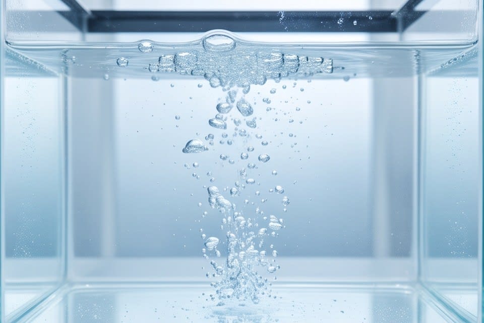
According to a study published in the Korean Journal of Chemical Engineering in 2022, acoustic vibration generated in microbubble arrays creates jet flow velocities of up to 148.5mm/s and removes particles from semiconductor surfaces with 92.5% efficiency. This figure shows that cleaning is not simply a sanitation process, but a key variable that determines semiconductor reliability. As package structures become more complex, the required precision of cleaning technology is also increasing, and within this trend, which technologies create a real difference has become a central question for the industry.
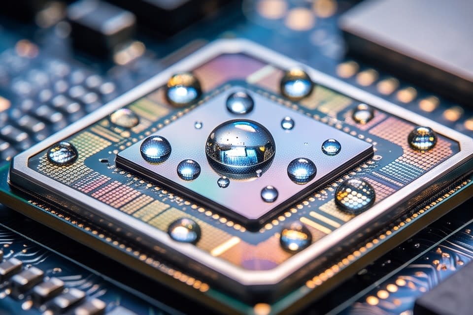
Technical demands that fine package structures place on the cleaning process
As semiconductor packages become more advanced, the technical burden placed on the cleaning process grows rapidly. Packages with fine pitch structures, such as FCBGA and WLCSP, leave flux residues and contaminant particles deep inside narrow capillary-like spaces after solder reflow. If these residues are not completely removed, electrical reliability may be compromised, directly affecting long-term service life.
The issue is that as structures become more precise, simply increasing cleaning energy can instead raise the risk of structural damage. Without controlling bubble cavitation, it is difficult to strike a balance between cleaning efficiency and structural preservation. Nanobubbles function by increasing heterogeneous nucleation on the surface, reducing adhesion between contaminants and the surface. This principle opens the possibility of removing fine particles without physical impact.
This is why the direction of cleaning technology is shifting from simple high-power methods to precise physicochemical control. Process results are determined by the mechanism used to separate particles.
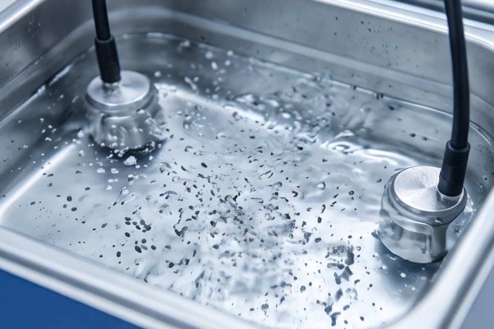
Process quality control created by combining ultrasonic dispersion and vision inspection
The reason ultrasonic dispersion technology is gaining attention in cleaning processes is not simply because it applies vibration energy. The key lies in reducing quality variability across the process by uniformly dispersing material particles in liquid at the micro level. In polishing processes as well, it has been confirmed that achieving uniform particle distribution through ultrasonic dispersion can prevent scratches and defects caused by excessive particles.
In highly integrated electronic components such as MLCC and FPCB, this uniformity is directly linked to assembly reliability. If the cleaning solution does not act uniformly, cleaning results vary by component, and that variation leads directly to lower yield. When a vision inspection algorithm is added, defects in fine patterns can be detected in real time, creating a structure that blocks defects before they move on to the next process.
Unlike when the two technologies operate independently, process feedback speed changes when dispersion control and defect detection occur simultaneously. Process improvement becomes possible only when data can track when and where defects occur. Securing both the uniformity of dispersion and the real-time capability of inspection is the key to cleaning processes for highly integrated components.
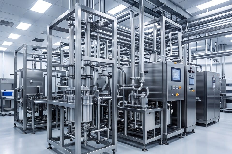
Impact of the Huvics laminator system on production efficiency and yield
The Huvics laminator system integrates the core lamination processes from Expander to Tape Mounting and UV Curing into a single line. It is structured to reduce transfer errors and waiting time that occur when processes are operated separately, while minimizing quality variation between each stage. Since production time in PCB lamination can vary from several hours to several days depending on optimization, the time-saving effect brought by process integration is difficult to ignore.
In the cleaning process, a multi-stage method applies Micro Bubble, Water Jet, and Air Knife step by step to remove surface contamination from components with different shapes, including camera modules, sensors, VCM motors, and trays. With a built-in Oven Dry function, the system is designed to complete drying after cleaning on the same line, reducing the risk of contamination reentry that can occur when separate external drying equipment is operated.
With selectable Lamp and LED UV Curing methods, the system flexibly responds to product groups with different requirements for adhesive strength and process stability. Since both Full Auto and Manual options are available, the same process design can be applied to lines with different production scales or automation levels. In advanced component manufacturing sites, equipment design is moving toward reducing process steps while maintaining the quality standards of each stage.
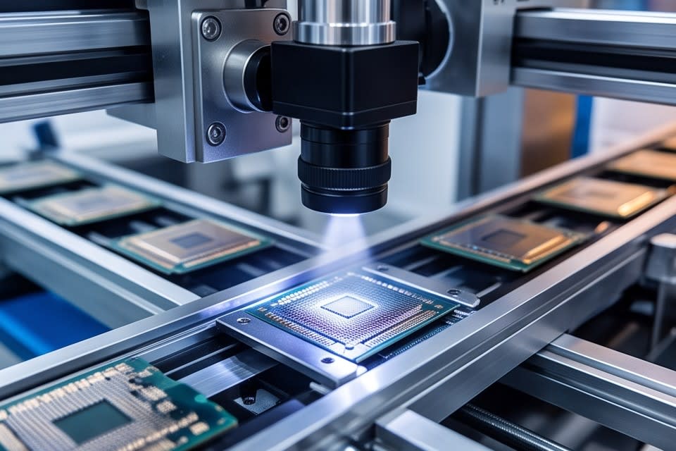
As semiconductor packages become thinner and more densely packed, the precision standards required of cleaning processes continue to rise. In a structure where even a single residue left in a fine space can compromise the reliability of an entire component, the principles of cleaning technology and process design are not a matter of choice, but a matter of yield. The reason the market is now paying close attention to semiconductor cleaning technology is that quality stability can only be secured when the uniformity of ultrasonic dispersion, the real-time capability of vision inspection, and the efficiency of process integration work together.
Huvics is an advanced technology company that develops and manufactures automation equipment and
production systems across the semiconductor, LED, Mobile, and Cosmetic industries.
With top talent and continuous technological innovation, we help customers improve productivity and
secure quality competitiveness.
Huvics Contact
Phone: 031-374-8285
Email: cdpark@huvics.com