Until now, many manufacturing sites have focused on increasing machining precision while placing cleaning and process integration at a lower priority. Even if equipment performance is improved, if the connection between processes is broken or microscopic contamination remains in the cleaning stage, the precision achieved with great effort cannot translate into yield. Now is the time for an approach that designs machining, cleaning, and process integration as one continuous flow.
Why ultra precision machining has become a basic requirement in modern manufacturing
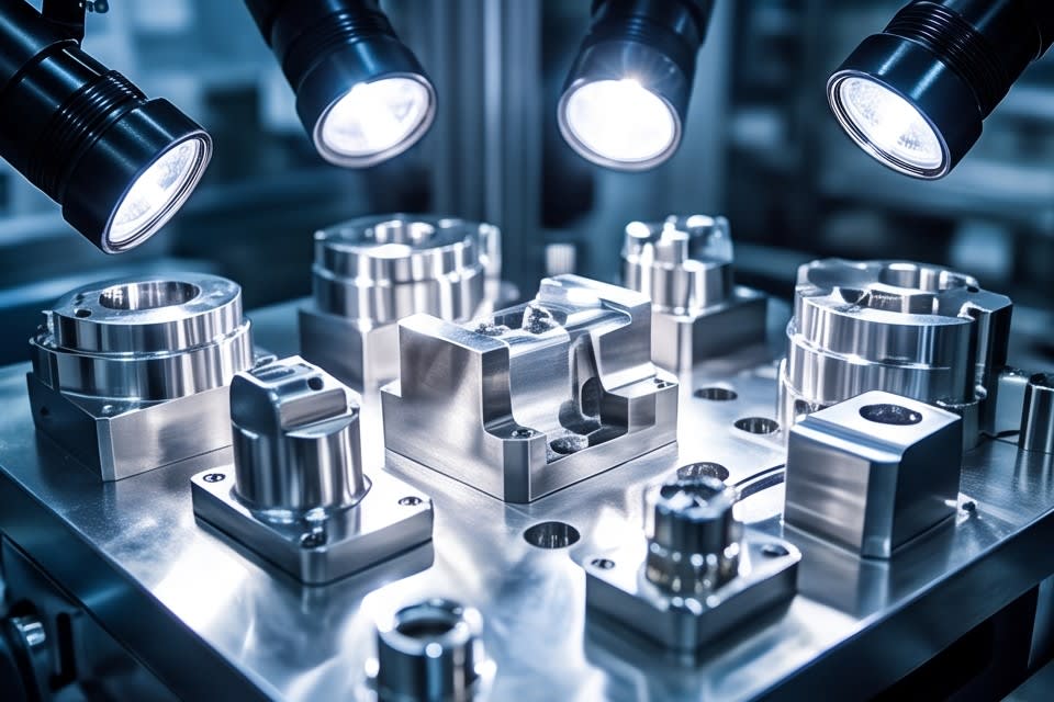
As semiconductor packaging technology advances, the allowable range of machining error continues to narrow. In the past, tolerances of several tens of microns were sufficient, but in structures that vertically stack dozens of chips, such as AI semiconductors and high performance memory, the uniformity of package thickness determines the reliability of the entire product.
Ultra precision machining operates at tolerance levels of ±0.001mm, or 1 micron, or less, and the latest research is expanding into areas that require dimensional tolerances below 10 nanometers and atomic level surface smoothness. As package types become more diverse, including FCBGA, WLCSP, and QFN·DFN, the grinding precision required for each structure also varies.
When errors invisible to the eye accumulate within a stacked structure, they affect both the electrical characteristics and mechanical durability of the final product. This is not simply a matter of equipment performance, but an issue across the entire process design. Grinding methods that combine diamond wheels with high precision stages have evolved to maintain stable quality even during high speed processes in order to meet these requirements. The trend is already clear: securing machining precision is no longer an option in modern manufacturing, but a basic requirement.
How the cleaning process determines yield and quality reliability
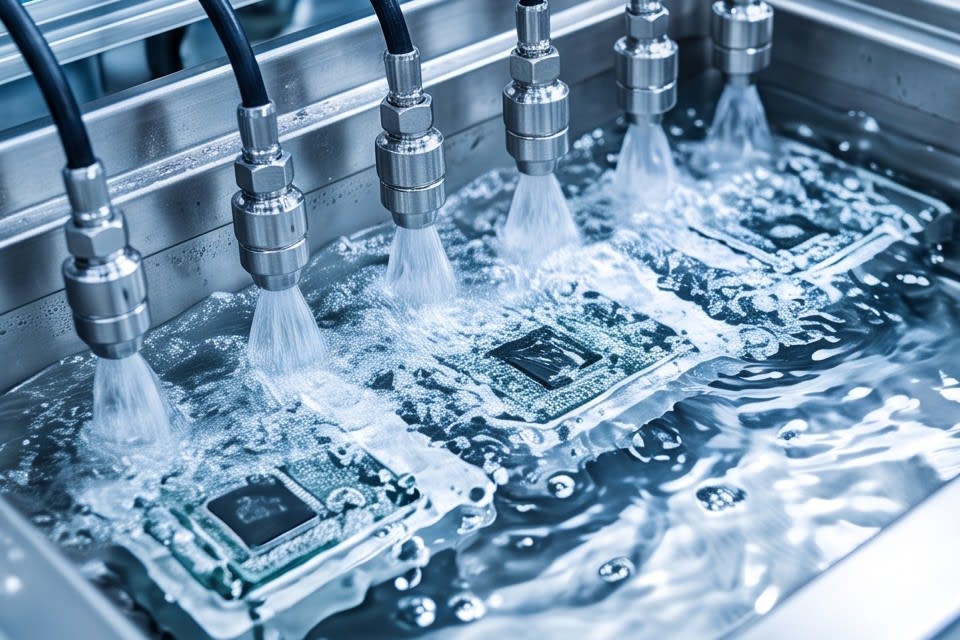
No matter how high machining precision becomes, yield collapses if microscopic contamination remains in the cleaning stage. Particle Removal Efficiency, or PRE, a key metric used in semiconductor cleaning processes, is a standard that numerically indicates how much contaminant particles have been removed from the surface of wafers or components. According to TSI analysis, particles left behind due to insufficient cleaning can cause critical defects in later processes, and continuous PRE monitoring is essential for maintaining yield and minimizing defects.
Research findings show that particle removal efficiency typically reaches more than 99%, but decreases to around 94% for ultrafine particles at the 0.064 micron level. As particle size becomes smaller, removal difficulty increases, and the design of the cleaning method must become more precise.
A multi stage cleaning method that combines micro bubbles, water jet, and air knife is a technical approach for responding to this ultrafine contamination, delivering effectiveness across a wider range of particle sizes than a single method. The drying process after cleaning also plays an important role in preventing contamination from reattaching, and if this stage is incomplete, the cleaning effect is reduced. For components where surface cleanliness is directly linked to performance, such as camera modules, autonomous driving sensors, and VCM motors, the design level of the cleaning process becomes the key factor that determines final quality.
Process design that connects grinding, lamination, and cleaning into one flow
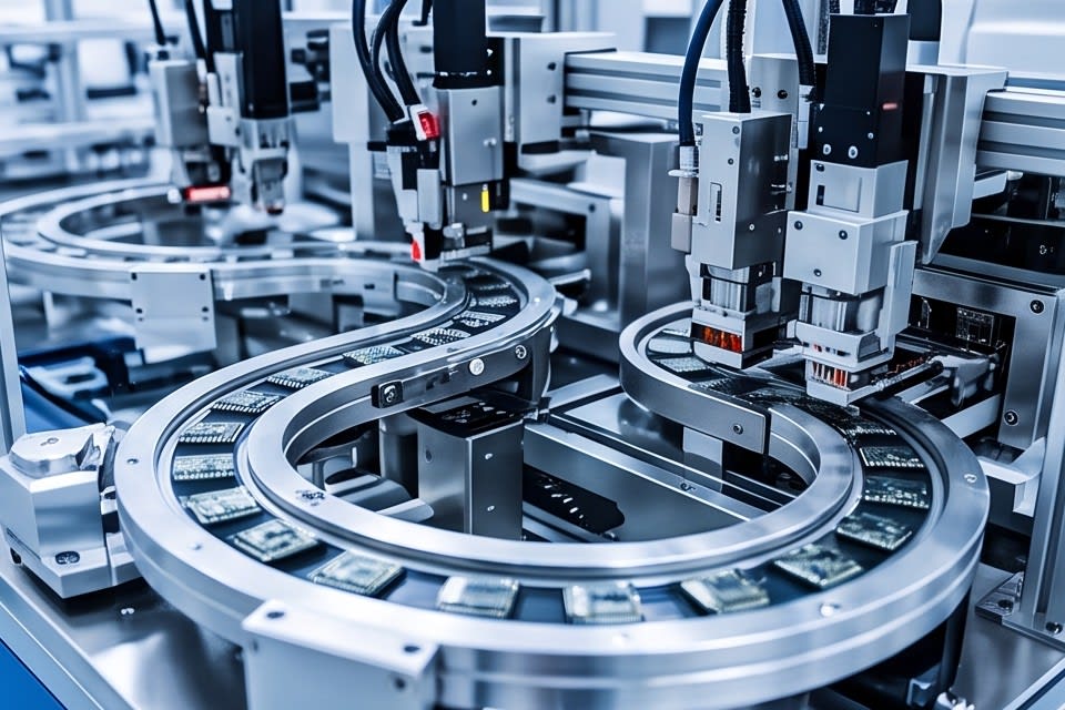
Anyone responsible for a manufacturing site knows well that process defects rarely originate from a single cause. Defects in the semiconductor tape bonding process may be problems with the bonding itself, but they are also often caused by surface conditions before attachment or mismatched UV curing conditions. Tray cleaning challenges also cannot be solved simply by replacing cleaning equipment unless contamination types and material characteristics are considered together. In this way, process defects are often not problems of one specific stage, but occur across the entire connected flow.
Based on this field context, Huvics adopts a method of designing grinding, lamination, cleaning, and drying processes as one flow. A one stop lamination process that continues from the Expander to UV curing reduces gaps between process stages to shorten tact time, the unit time required to produce one product, and enables an integrated response to issues involving complex causes, such as improving the defect rate of camera modules. The ability to flexibly select Full Auto and Manual configurations also makes it possible to adjust solutions to the practical conditions of the production line. These cases show where the starting point lies for reducing defects already anticipated in process design.
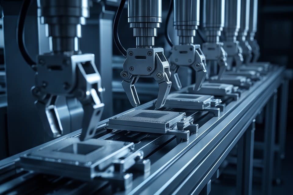
Machining precision, cleaning efficiency, and process integration may seem like separate tasks, but in actual manufacturing sites they are one connected issue. Securing micron level grinding tolerances, designing a cleaning process that removes even ultrafine particles, and connecting each stage without interruption is the way to increase both yield and quality reliability. For manufacturing to maintain a technological edge in global competition, it needs a perspective that views these three elements as one continuous flow.
Huvics is an advanced technology company that develops and manufactures automation equipment and
production systems across the semiconductor, LED, Mobile, and Cosmetic industries.
With top talent and continuous technological innovation, we support customers in improving productivity and
securing quality competitiveness.
Huvics Contact Information
Phone: 031-374-8285
Email: cdpark@huvics.com