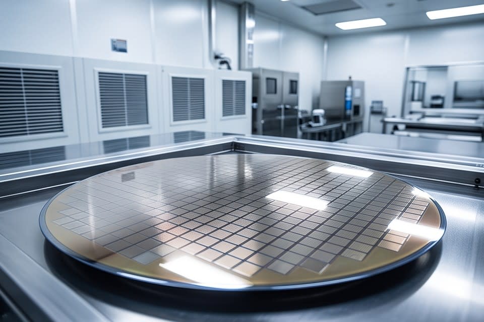
A semiconductor process is like an operating room. Just as a scalpel moves in micron units and a tiny foreign particle left on a surgical tool can change a patient outcome, a single particle left during the process can determine the fate of an entire chip. An environment where cleanliness becomes the prerequisite for technology, this is the reality of today's semiconductor manufacturing sites.
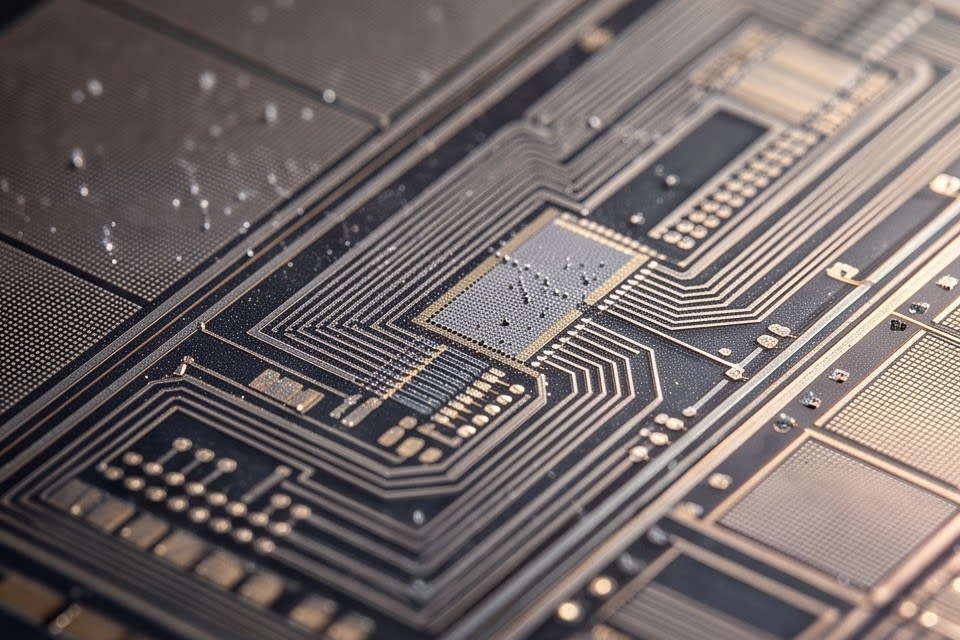
As nodes shrink, the impact of contaminant particles grows
In semiconductor processes, the impact of contaminant particles on yield increases nonlinearly as nodes become smaller. In a 28nm process, a 1 micrometer particle is treated as practically harmless because the chance of colliding with circuit patterns is low. However, according to an analysis by Applied Physics USA, a particle of the same size becomes a critical defect source in a 5nm process because it exceeds the circuit line width itself.
During the photolithography stage, even a single fine particle settling on the wafer surface can make the entire die subject to disposal. Particles smaller than 0.5 micrometers penetrate into areas that are difficult even to detect with conventional contamination control methods.
The relationship between defect density and yield is also clear in numerical terms. Patent literature confirms that in a 1 gigabit DRAM process, reducing defect density from 0.10 Defects/cm² to 0.01 Defects/cm² raises process yield from 12% to 81%. As process miniaturization advances, the threshold for acceptable contamination levels becomes lower, and cleaning is emerging as a structure that directly determines yield.
Why cleaning has become a core process
The status of cleaning on the production floor has changed because the process structure itself has changed. In the past, cleaning was considered a final step that removed foreign matter from the product surface. However, in sites where complex structures and materials coexist, such as camera modules, semiconductor trays, and tape bonding processes, contamination control is required at every intermediate process stage.
Advanced packaging methods such as WLCSP, which remove the substrate and mount the die directly on the main PCB, reduce process steps but require higher cleanliness at each step. Because there is no structural margin to compensate for differences in thermal expansion coefficients between silicon and substrate materials, fine foreign matter left on the bonding surface leads directly to reliability issues.
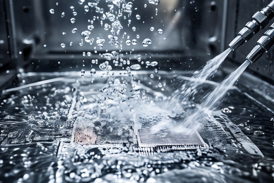
This is also why multi-stage cleaning technology is attracting attention. A cleaning method that combines Micro Bubble, Water Jet, and Air Knife separates and treats contaminant particles by stage, including types that are difficult to remove with a single method. When an oven drying function is also installed, the possibility of secondary contamination caused by residual moisture after cleaning is blocked as well. Which combination of cleaning technologies is selected becomes the key turning point for final quality stability.
Precision machining and cleaning form one quality management system
Precision machining and cleaning should be understood not as independent processes, but as one continuous quality management system. When processing advanced packages with extremely high requirements for thickness uniformity and flatness, such as FCBGA, WLCSP, QFN, and DFN, the precision of the grinding process alone cannot guarantee completion quality.
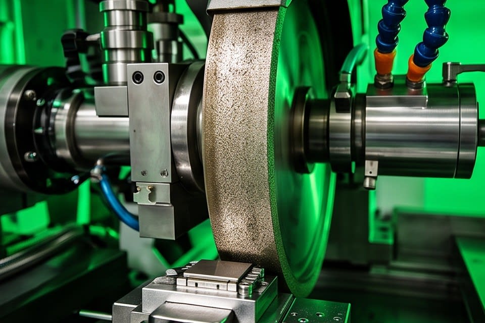
Even when micron-level grinding is performed using a diamond wheel and a high-precision stage, grinding byproducts and fine particles remaining on the surface after machining act as contamination sources in the next process. Huvics PKG Grinder is equipment designed to meet these ultra-precision grinding requirements, and yield and reliability can be secured at the same time when process design linked through the cleaning stage after grinding is reviewed together.
As machining precision increases, the allowable range for residual contamination becomes even narrower, and the role of cleaning expands to fill that gap. This is where the significance of the proposition that precision machining and cleaning must be designed together as processes become more miniaturized can be confirmed.
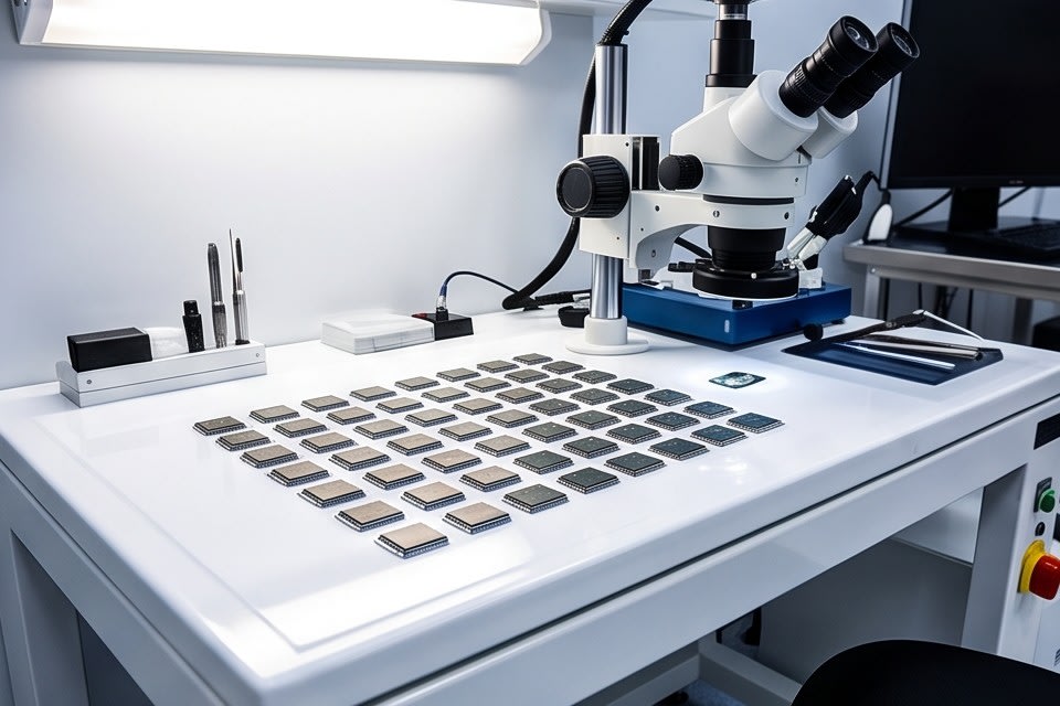
Just as cleanliness in an operating room is as important as surgical skill, cleaning in semiconductor manufacturing carries the same weight as process technology. As nodes shrink and packages become thinner, the margin for allowable contamination disappears. Only when cleaning is viewed as the starting point of process design can meaningful improvements in yield and reliability begin.
Huvics is an advanced technology company that develops and manufactures automation equipment and
production systems across the semiconductor, LED, Mobile, and Cosmetic industries.
With outstanding talent and continuous technological innovation, we support customers in improving productivity and
securing quality competitiveness.
Huvics Contact
Phone: 031-374-8285
Email: cdpark@huvics.com