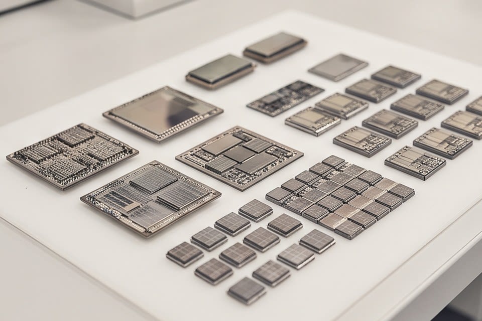
In the semiconductor industry, 'packaging' was long regarded as a finishing step placed behind design and process work. However, as demand for AI accelerators and high-performance memory has surged, the situation has changed rapidly. Product competitiveness now depends not only on the performance of a single chip, but on how precisely multiple chips are stacked and connected. Packaging technology now stands at the center of a technology race as intense as semiconductor design itself.
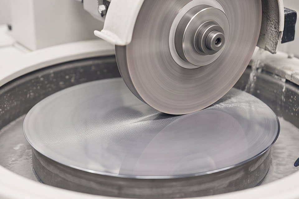
Why Ultra-Precision Grinding Determines Yield
High-bandwidth memory used in AI accelerators must process more than 1TB of data per second through a vertically stacked structure. To meet this requirement, each stacked chip must have uniform thickness, and surface flatness must also be controlled at the micron level. According to Mordor Intelligence, 3D stacked memory accounts for 34.28% of revenue share in the advanced semiconductor packaging market as of 2025, establishing itself as the leading technology.
As package formats diversify, such as FCBGA, WLCSP, and QFN, thickness precision standards also vary by type. For example, WLCSP requires a fine pitch between 0.3mm and 0.5mm. Ultimately, grinding precision in the packaging process is a key variable that determines yield. Even a slight increase in thickness variation can undermine the electrical reliability of the entire stacked structure, directly leading to performance degradation in the final product.
Huvics PKG Grinder responds to these standards with micron-level grinding using a diamond wheel. It is available in both Full Auto and Manual configurations, allowing flexible application according to the production line structure of each customer, while maintaining stable quality even in high-speed processes to achieve high yield. Machining precision is product reliability is the principle that most clearly explains the role this equipment plays in semiconductor packaging processes.
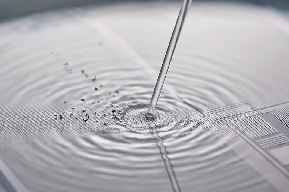
Why the Cleaning Process Is the Starting Point of Quality
If grinding determines the form of packaging, cleaning is the process that ensures this form can perform its intended function. A single fine particle remaining on the semiconductor surface can contaminate the entire subsequent process or lead to defects in the final product. Especially in components that require optical precision, such as camera modules or autonomous driving sensors, invisible contamination can quietly erode product reliability. This is why the cleaning process must be treated not as simple washing, but as the starting point of quality stability.
Huvics Cleaner System removes contaminant particles from product surfaces by sequentially combining Micro Bubble, Water Jet, and Air Knife, and consistently handles the drying process through its Oven Dry function. Cleaning conditions can be configured differently according to product types such as camera modules, sensors, VCM motors, and trays, enabling a single system to address diverse process requirements.
In practice, many cases have shown that defects occurring in semiconductor tape bonding processes and yield loss in camera modules can be resolved by improving the cleaning process. Reducing particles reduces defects, and reducing defects increases yield. Engineers who have worked with cleaning processes know well how difficult it is to implement this simple connection in the field. The significance of precision cleaning is confirmed by the fact that it is not the end of the process, but the foundation of quality.
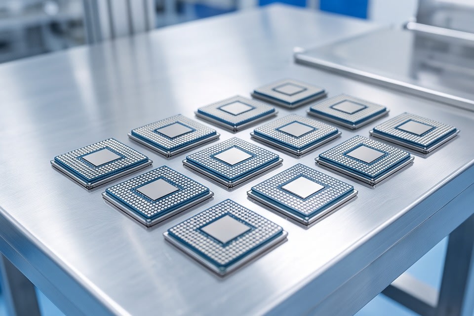
The competition in semiconductor packaging technology is now shifting toward process precision as much as chip design. Grinding and cleaning are the two pillars that support yield and reliability in this competition. If either one becomes unstable, even the most sophisticated package design will struggle to deliver its intended performance in the field. In an era when technological precision becomes product competitiveness, how firmly each and every process is built will ultimately determine a company's position in the future semiconductor market.
Huvics is an advanced technology company that develops and manufactures automation equipment and
production systems across the semiconductor, LED, Mobile, and Cosmetic industries.
With top talent and continuous technological innovation, we support customers in improving productivity and
securing quality competitiveness.
Huvics Contact
Tel: 031-374-8285
Email: cdpark@huvics.com