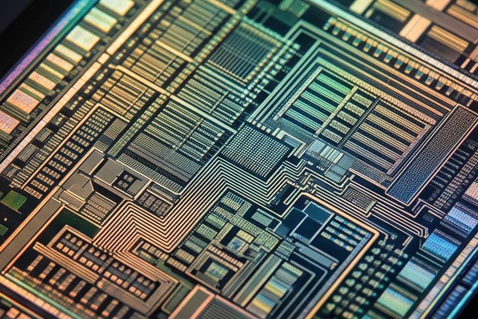
According to data from Semiconductor Equipment and Materials International (SEMI), a significant share of defects in semiconductor processes is reported to originate from particle contamination. This means that a single particle just a few micrometers in size, invisible to the naked eye, can undermine the yield of an entire chip. As processes become more miniaturized and package structures grow more complex, the precision of each stage, including cleaning, drying, grinding, and lamination, is emerging as a key factor that determines final product quality. By examining which technologies control these variables, we can see the direction in which digital transformation in semiconductor manufacturing is moving.
Structure and Principles of a Multi-Stage Cleaning and Drying System
Contaminants remaining on semiconductor surfaces are especially difficult to handle because they are not visible. Fine contamination made up of organic matter, metal residues, and particles is difficult to remove through simple physical washing. The approach developed to solve this problem is multi-stage cleaning technology.
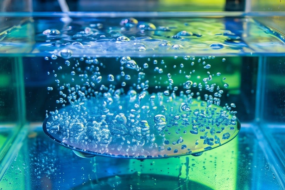
According to a study published in the Korean Journal of Chemical Engineering, a cleaning system using acoustic bubble arrays was shown to remove fine particles of various wettability and sizes with an efficiency of 92.5%. Microbubbles are generated at sizes of 5 nm or less, physically and chemically separating oils and fine particles from the substrate surface, while the following water jet pushes away suspended contaminants. In the air knife stage, remaining moisture and particles on the surface are removed by airflow, and the final oven drying process completely evaporates any moisture left after cleaning.
Huvics' 4-stage cleaning and drying system is designed to process this sequence within a single line. For automotive electronics components such as camera modules or autonomous driving sensors, which require both optical cleanliness and electrical reliability, a structure that continuously controls the process through drying is especially important. This is because residual moisture can lead to poor adhesion or corrosion in subsequent processes. The industry is shifting from a method that separated cleaning and drying into individual processes toward an integrated inline system.
Grinding and Lamination That Improve Package Process Precision
As demand for AI semiconductors and high-performance memory increases, package structures are becoming increasingly complex. This is because the mainstream is shifting away from enclosing a single chip in encapsulant and toward structures that vertically stack multiple chips. This change is fundamentally raising the requirements for the grinding process.
Thickness Uniformity in the Grinding Process
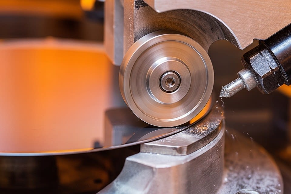
In stacked packages, even a thickness deviation of only a few micrometers in each layer can directly lead to electrical connection defects or heat dissipation issues. According to published data from the patent office, rough grinding in the package grinding process takes about 2.5 to 5 minutes, while finish grinding takes about 2 to 4 minutes. The key is achieving the target thickness uniformly within this short time. Because required thickness and surface roughness differ by package type, such as FCBGA, WLCSP, and QFN/DFN, equipment must be able to combine diamond wheels with high-precision stages and set conditions differently at the micron level.
Integrated Structure of the Lamination Process
The same applies to the lamination process. If equipment is changed at each stage from tape mounting to UV curing, alignment errors accumulate between processes. To reduce this, a one-stop structure that processes everything from the expander to UV curing within a single system is being introduced. How well the processes can be integrated and how precisely the conditions of each stage can be controlled is the key factor that determines next-generation package yield.
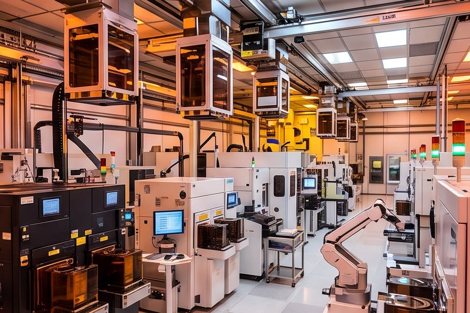
Cleaning, grinding, and lamination may appear to be independent processes, but these three stages are connected as one quality chain. If the surface is not completely cleaned, grinding precision becomes unstable, and if thickness after grinding is not uniform, lamination adhesion becomes uneven. Digital transformation in semiconductor manufacturing is not an abstract concept. It begins with precisely controlling each of these connected links through data and automation.
Huvics is an advanced technology company that develops and manufactures automation equipment and
production systems across the semiconductor, LED, Mobile, and Cosmetic industries.
With top talent and continuous technological innovation, we support customers in improving productivity and
securing quality competitiveness.
Huvics Contact
Tel: 031-374-8285
Email: cdpark@huvics.com