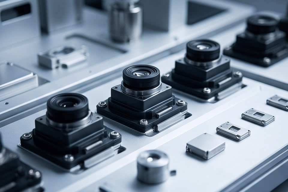
In the past, the cleaning process for semiconductor components was regarded as a supporting task that simply washed away foreign matter. However, as component integration has increased and package structures have become more complex, the cleaning process has emerged as a key variable that determines yield and reliability. Now that components such as MLCC, FPCB, and camera modules, which require micron-level tolerances, have become mainstream, the scope and precision that cleaning technology must handle have fundamentally changed.
The new standards for cleaning technology shaped by miniaturization and high integration
The miniaturization and high integration of semiconductor components have changed the very nature of contamination that the cleaning process must address. In an environment where a single particle of several tens of micrometers or less can lead to pattern shorts or bonding defects, simple spraying of cleaning solution is not enough to control surface contamination sufficiently.
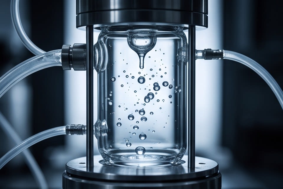
According to a study published in the Korean Journal of Chemical Engineering, a cleaning method using a micro bubble array achieved a cleaning efficiency of up to 92.5% and produced a jet velocity up to 5 times higher than that of a single cylinder structure. As the precision of the physical cleaning mechanism increases, particle removal efficiency rises as well.
In manufacturing sites for ultra precision components such as camera modules, sensors, and VCM motors, the surface condition after cleaning directly affects the final assembly yield. As process environments become more demanding, the criteria for selecting cleaning technology must go beyond simple specification comparisons. Across the industry, the combination of cleaning methods is increasingly determined by the type of contamination being handled as well as the shape and material of the component.
The combination of ultrasonic dispersion and vision inspection
One of the keys to improving the precision of the cleaning process lies in how uniformly particles in the liquid phase can be controlled. If particles agglomerate or become unevenly distributed in the cleaning solution, the cleaning energy applied to the surface becomes inconsistent, leaving contamination in specific areas.
This is also why frequency selection is important in ultrasonic cleaning. For substrates with integrated precision circuit patterns such as FPCB, frequencies in the 35~40kHz range are suitable because they provide gentle cleaning energy while effectively separating fine contaminant particles.
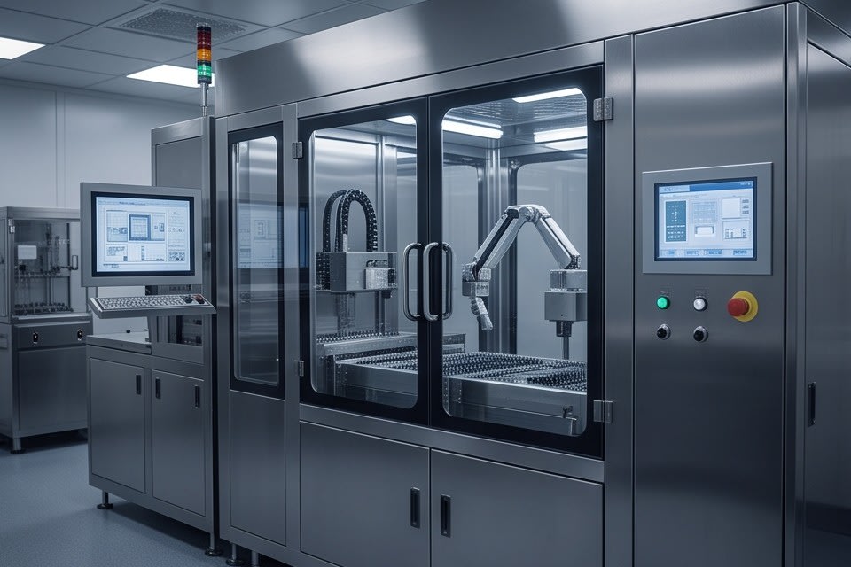
Huvics' independently developed ultrasonic dispersion technology uniformly disperses material particles in the liquid phase at the micron level, stabilizing the physical properties of materials. When combined with vision inspection algorithms, it detects defects in remaining fine patterns after cleaning in real time and prevents defective products from moving on to the next process.
Just as the uniformity of particle dispersion in the MLCC process leads directly to the stability of electrical characteristics, cleaning technology and inspection technology must operate within a single loop to substantially control quality variation. Whether the two technologies exist independently or are organically connected within the process flow is the key criterion in selecting a cleaning solution.
The multi stage structure of the Cleaner System and criteria for application decisions
The choice of cleaning method depends on the product shape, contamination type, and production scale. In structures where lenses and sensors are positioned close together, such as camera modules, the penetration path and discharge direction of the cleaning solution must be precisely designed. For components with large surface areas and complex shapes, such as semiconductor trays, a multi stage cleaning method is advantageous.
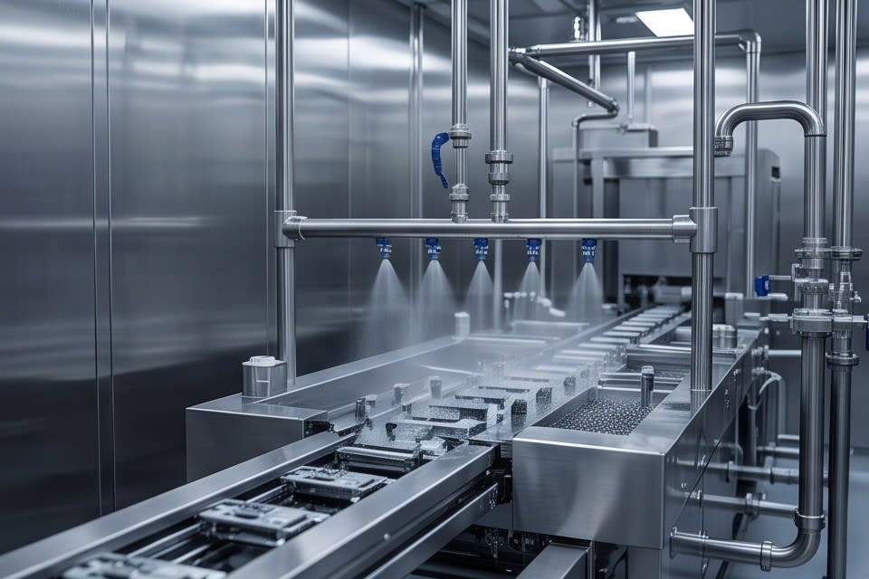
The Huvics Cleaner System is composed of a multi stage cleaning structure that combines Micro Bubble, Water Jet, and Air Knife, and it completes the process flow through drying with an Oven Dry function at the end of the line. According to industry cases, processes that introduced UHP water jet cleaning reported a 40% reduction in cleaning preparation time. With both Full Auto and Manual options, the line can be configured according to production scale and automation level.
Rather than looking only at cleaning efficiency, it is worth considering an approach that also designs the surface condition after drying and the connection with subsequent processes.
The impact of integrated lamination processes on packaging quality
The lamination process determines the quality of semiconductor packaging from a direction different from cleaning. When tape or protective film is precisely attached to a wafer or substrate, bubbles, wrinkles, or uneven adhesion can affect the entire subsequent process.
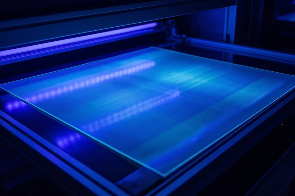
In particular, UV curing is a step that must secure both adhesive strength and process stability, and curing speed and energy uniformity determine the production rhythm of the entire line. Analyses suggest that semi automatic laminators can improve productivity by up to 50% compared with manual feeding, but as the level of automation increases, process linkage design between equipment becomes more important.
The Laminator System is designed to integrate key processes from Expander to Tape Mounting and UV Curing within a single system, reducing errors that occur during transfer between processes. Lamp and LED type UV Curing can be selectively applied, allowing curing conditions to be optimized according to component characteristics and adhesive materials.
Integrating processes does not simply mean reducing the number of equipment units. It means reducing variables between each step and improving the reproducibility of quality, and this is where the significance of integrated lamination design becomes clear.
Cleaning and lamination may seem like separate processes, but ultimately they pursue the same goal. They control the surface condition and prepare the next process to begin under optimal conditions. As semiconductor components become smaller and more complex, the precision of this preparation carries greater weight in determining overall yield. What today's manufacturing sites require is not merely choosing a specific technology, but designing the entire process as one continuous flow.
Huvics is an advanced technology company that develops and manufactures automation equipment and
production systems across the semiconductor, LED, Mobile, and Cosmetic industries.
With top talent and continuous technological innovation, Huvics supports customers in improving productivity and
securing quality competitiveness.
Huvics Contact
Phone: 031-374-8285
Email: cdpark@huvics.com